
The AD9066 is a dual 6-bit ADC that has been optimized for low-cost in-phase and quadrature (I and Q) demodulators. Primary applications include digital direct broadcast satellite applications where broadband quadrature phase shift keying (QPSK) modulation is used. In these receivers, the recovered signal is separated into I and Q vector components and digitized. To reduce total system cost and power dissipation, the AD9066 provides an internal voltage reference and operates from a single +5 volt power supply. Digital outputs are CMOS compatible and rated to 60 MSPS conversion rates. The digital input (ENCODE) utilizes a CMOS input stage with a TTL compatible (1.4 V) threshold. The AD9066 is housed in a 28-lead SOIC and a 28-lead SSOP package and is available in two temperature grades. The AD9066JR is rated for operation over the 0°C to 70°C commercial temperature range. The AD9066AR/ARS is rated for the –40°C to +85°C industrial temperature range.
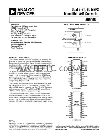
The AD9066 is a dual 6‑bit analog‑to‑digital converter optimized for low‑cost I/Q demodulators used in direct broadcast satellite receivers, QAM demodulators, wireless LANs and VSAT receivers. It operates from a single +5 V supply, provides an internal voltage reference, and offers CMOS‑compatible digital outputs rated up to 60 MSPS.
Available in 28‑lead SOIC and SSOP packages, the device supports both ac‑coupled and dc‑coupled inputs, with a typical full‑scale input range of 500 mV. Detailed specifications include power dissipation of 400 mW, ENOB of up to 5.7 bits, and extensive pin‑out and timing information for system designers.
| Resolution | 6 bits (dual) |
|---|---|
| Supply Voltage | +5 V |
| Power Dissipation | 400 mW (typical) |
| Full‑Scale Input Range | 500 mV |
The AD9066 operates from a single +5 V supply.
It is offered in 28‑lead SOIC and 28‑lead SSOP packages.
Typical power dissipation is 400 mW.