
OP177 is an ultra-precision operational amplifier that features ultra-low output offset voltage and offset voltage drift.
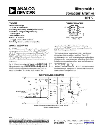
The OP177 is an ultralow‑offset, bipolar‑input operational amplifier offering 25 µV maximum offset voltage at 25 °C and a drift of only 0.1 µV/°C. It delivers high open‑loop gain, low supply current (2 mA max), and excellent CMRR (≥130 dB) and PSRR (≥115 dB) in both PDIP and SOIC packages.
The document includes detailed pin configurations, functional block diagrams, absolute maximum ratings, thermal resistance data, and typical performance curves such as gain linearity, noise versus frequency, and temperature effects. Electrical characteristics are presented for the OP177F and OP177G variants.
| Input Offset Voltage (Vos) | 25 µV max (typical 10 µV) |
|---|---|
| Input Offset Voltage Drift (TCVos) | 0.1 µV/°C max |
| Input Bias Current (Ib) | 0.2 nA typical, 2 nA max |
| CMRR | ≥130 dB |
| PSRR | ≥115 dB |
| Supply Current (Is) | 2 mA max at +15 V |
| Power Consumption (Po) | 60 mW max at +15 V |
The OP177 has an input offset voltage of up to 25 µV at room temperature.
The device draws up to 2 mA of supply current with a +15 V supply and no load.
The absolute maximum supply voltage is +22 V.