
The AD8557 is a zero drift, sensor signal amplifier with digitally programmable gain and output offset. Designed to ease the design of sensor signal conditioning and amplification applications, the AD8557 features very low offset voltage, input offset voltage drift, and CMRR. The AD8557 is ideal for sensor applications such as automotive sensors, pressure and position sensors, precision current sensing, thermocouple amplifiers, industrial weigh scales, and strain gages.
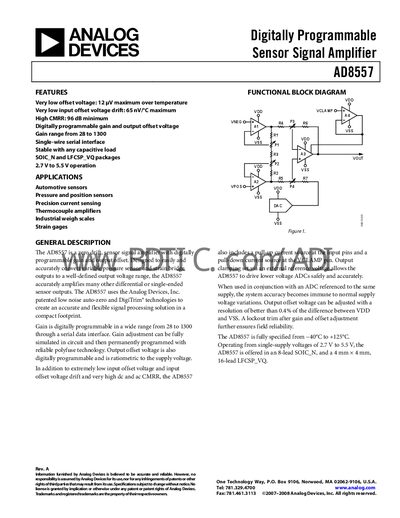
The AD8557 is a digitally programmable sensor signal amplifier with very low offset voltage (2 µV min, 12 µV typ) and low drift (65 nV/°C max). It offers a gain range of 28 to 1300, programmable via a single‑wire serial interface, and operates from a single‑supply voltage of 2.7 V to 5.5 V in 8‑lead SOIC_N or 16‑lead LFCSP_VQ packages.
The document provides features, applications (automotive sensors, pressure and position sensors, etc.), functional block diagrams, detailed specifications (input bias current, CMRR, PSRR, thermal resistance), absolute maximum ratings, pin configurations, and typical performance graphs.
| Input Offset Voltage | 2 µV min, 12 µV typ, 20 µV max |
|---|---|
| Input Offset Voltage Drift | 65 nV/°C max |
| Common‑Mode Rejection Ratio (CMRR) | 96 dB min |
| Supply Voltage Range | 2.7 V to 5.5 V |
| Operating Temperature Range | -40 °C to +125 °C |
| Gain Bandwidth Product | 2 MHz (first stage), 8 MHz (second stage) |
The AD8557 provides a digitally programmable gain range from 28 to 1300.
It operates from a single‑supply voltage of 2.7 V to 5.5 V.
The device is offered in 8‑lead SOIC_N and 16‑lead LFCSP_VQ packages.
The input offset voltage drift is specified up to 65 nV/°C.