
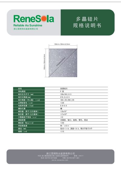
This document provides the technical specifications for ReneSola multi‑crystalline silicon wafers. It includes physical dimensions, thickness tolerances, impurity concentrations, and defect limits for the wafers produced by Zhejiang Renesola Solar Energy Co., Ltd.
Key parameters such as wafer size (156 mm × 156 mm), thickness (180 µm ± 20 µm), carbon content, and allowable defect counts are listed, allowing manufacturers and engineers to assess suitability for photovoltaic module production. This manual is written in Chinese.
| Wafer thickness (center value) | 180 µm ±20 µm |
|---|---|
| Total thickness variation | ±30 µm |
| Carbon impurity concentration | 8 × 10⁷ atoms/cm³ |
| Other impurity concentration | 7 × 10¹⁸ atoms/cm³ |
| Minority carrier lifetime | 2 µs |
| Maximum edge defect count per wafer | < 50 |
| Wafer verticality tolerance | 90° ± 0.5° |
| Edge roughness (length) | < 1.0 mm |
| Line defect count per wafer | < 15 |
The carbon content is 8 × 10⁷ atoms per cubic centimeter.
The wafer thickness is 180 µm ± 20 µm, with a total thickness variation of ±30 µm.