
MRF7S15100HR3 is a N-Channel Enhancement-Mode Lateral MOSFETs produced by Freescale Semiconductor. It is designed for CDMA base station applications with frequencies from 1470 to 1510 MHz, and can be used in Class AB and Class C for all typical cellular base station modulations.
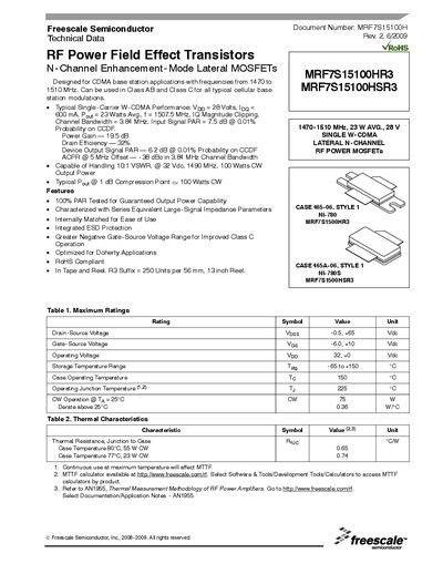
This Freescale datasheet describes the RF Power Field Effect Transistors MRF7S15100HR3 and MRF7S15100HSR3, N‑channel enhancement‑mode lateral MOSFETs designed for CDMA base‑station applications from 1470 MHz to 1510 MHz. It includes typical performance figures such as 28 V peak‑to‑peak voltage, 600 mA drain current, 23 W average output power, and 19.5 dB power gain.
The document also lists maximum ratings, thermal characteristics, electrical parameters, ESD protection data, and a complete test‑circuit schematic with component values. Revision history, related application notes, and links to Freescale software tools (including an MTTF calculator) are provided at the end.
| Drain‑Source Voltage (Voss) | -0.5 to +65 V |
|---|---|
| Gate‑Source Voltage (Ves) | -6.0 to +10 V |
| Operating Voltage (Vop) | 32 V |
| Power Gain | 19.5 dB |
| Drain Efficiency | 32 % |
| Typical Output Power (Pout) | 23 W Avg. |
| Frequency Range | 1470‑1510 MHz |
| Typical Single‑Carrier W‑CDMA Performance | Vpp 28 V, Ip 600 mA, Pout 23 W Avg., f 1507.5 MHz |
| Maximum CW Output Power (1 dB Compression) | ≈100 W CW |
| Case Operating Temperature | Up to 150 °C |
The device is rated for a drain‑source voltage from –0.5 V to +65 V.
At 1 dB compression the transistor can deliver about 100 W continuous wave.
The case can operate up to 150 °C.