
SN74LVT18502 and SN74LVT182502 are 3.3V ABT scan test devices with 18-bit universal bus transceivers. They support mixed-mode signal operation with 5V input and output voltages as well as 3.3V VCC. They can operate with unregulated battery voltages as low as 2.7V. The UBT (Universal Bus Transceiver) combines D-type latches and D-type flip-flops for operation in transparent, latched, or clocked mode. The bus-hold data inputs eliminate the need for external pullup resistors. The B-port outputs of SN74LVT182502 devices have equivalent 25-Ω series resistors, so no external resistors are required. They are compatible with the IEEE Standard 1149.1-1990 (JTAG) test access port and boundary-scan architecture. The SCOPE instruction set includes the required instructions of IEEE Standard 1149.1-1990 and optional CLAMP and HIGHZ instructions. It also supports parallel-signature analysis at inputs, pseudo-random pattern generation from outputs, sample inputs/toggle outputs, binary count from outputs, device identification, and even-parity opcodes. The devices are packaged in 64-pin plastic thin quad flat packages with 0.5-mm center-to-center spacings.
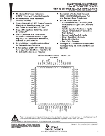
The SN74LVT18502 and SN74LVT182502 are 3.3‑V ABT scan test devices that belong to Texas Instruments' SCOPE™ testability family. They provide 18‑bit universal bus transceivers that can operate in transparent, latched, or clocked modes and support IEEE 1149.1‑1990 boundary‑scan.
The devices include an 8‑bit instruction register, four test‑data registers, and a 64‑pin Plastic Thin Quad Flat Package. They operate from –40 °C to 85 °C and feature bus‑hold circuitry, internal pull‑ups, and B‑port outputs capable of sourcing or sinking up to 12 mA.
| Operating voltage | 3.3 V Voc (supports 5 V TTL interface) |
|---|---|
| TTL interface capability | 5 V system environment |
| B‑port output current | Up to 12 mA source or sink |
| Operating temperature range | –40 °C to 85 °C |
| Package type | 64‑Pin Plastic Thin Quad Flat Package |
| Instruction register reset value | Binary 10000001 (IDCODE) |
Four dedicated test pins are used: TDI (test data input), TDO (test data output), TMS (test mode select), and TCK (test clock).
The instruction register resets to the binary value 10000001, which selects the IDCODE instruction.
The B‑port outputs can source or sink up to 12 mA.
The devices are specified to operate from –40 °C to 85 °C.