
NLSF3T126 is a high-speed CMOS quad bus buffer fabricated with silicon gate CMOS technology. It achieves non-inverting high-speed operation similar to equivalent Bipolar Schottky TTL while maintaining CMOS low power dissipation. The NLSF3T126 requires the 3-state control input (OE) to be set Low to place the output into high impedance. The T126 inputs are compatible with TTL levels. This device can be used as a level converter for interfacing 3.3 V to 5.0 V, because it has full 5.0 V CMOS level output swings. The NLSF3T126 input structures provide protection when voltages between 0 V and 5.5 V are applied, regardless of the supply voltage. The output structures also provide protection when VCC = 0 V. These input and output structures help prevent device destruction caused by supply voltage − input/output voltage mismatch, battery backup, hot insertion, etc. The internal circuit is composed of three stages, including a buffer output which provides high noise immunity and stable output. The inputs tolerate voltages up to 7.0 V, allowing the interface of 5.0 V systems to 3.0 V systems. Features • High Speed: tPD = 3.8 ns (Typ) @ VCC = 5.0 V • Low Power Dissipation: ICC = 4.0 µA (Max) @ TA = 25°C • TTL-Compatible Inputs: VIL = 0.8 V; VIH = 2.0 V • Power Down Protection Provided on Inputs • Balanced Propagation Delay
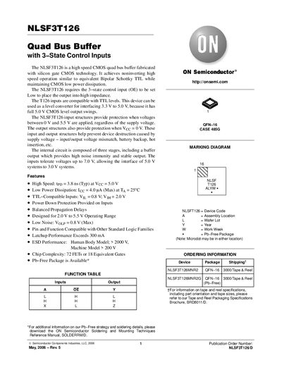
The NLSF3T126 quad bus buffer provides non‑inverting high‑speed operation with CMOS low power consumption. It features three internal stages, a high‑noise‑immunity output, and 3‑state control (OE) that places the output in high‑impedance when OE is low. The device is compatible with TTL input levels and can serve as a level converter between 3.3 V and 5 V systems.
Electrical specifications include a typical propagation delay of 3.8 ns at 5 V, low supply current (4 µA max), and operation over a 2.0 V to 5.5 V range. The package is a 16‑pin QFN with detailed mechanical dimensions and ordering information provided for tape‑and‑reel supply.
| Propagation Delay (tpp) | 3.8 ns typ at Vcc=5.0 V |
|---|---|
| Supply Current (Icc) | 4.0 µA max at 25 °C |
| TTL‑Compatible Input Thresholds | VIL ≈ 0.8 V, VIH ≈ 2.0 V |
| Operating Voltage Range | 2.0 V to 5.5 V |
| Maximum Output Current per Pin | 425 mA |
| Output Low Voltage (VOL) @ 50 mA | 2.0 V typical |
| ESD Performance | Human Body Model > 2000 V |
Set the 3‑state control input (OE) low.
Approximately 3.8 ns typ at Vcc = 5.0 V.
It operates from 2.0 V to 5.5 V.
VIL is about 0.8 V and VIH is about 2.0 V.