
Key facts
- Manuals
- 1
- Languages
- EN
- Last added
- 2012-01-04
Featured NLSF3T126 manuals
ON Semiconductor NLSF3T126 Quad Bus Buffer Datasheet
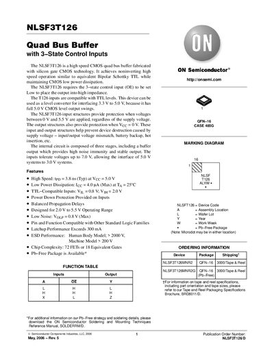
The NLSF3T126 quad bus buffer provides non‑inverting high‑speed operation with CMOS low power consumption. It features three internal stages, a high‑noise‑immunity output, and 3‑state control (OE) that places the output in high‑impedance when OE is low. The device is compatible with TTL input levels and can serve as a level converter between 3.3 V and 5 V systems.
Electrical specifications include a typical propagation delay of 3.8 ns at 5 V, low supply current (4 µA max), and operation over a 2.0 V to 5.5 V range. The package is a 16‑pin QFN with detailed mechanical dimensions and ordering information provided for tape‑and‑reel supply.
Covers: Features · Function Table · Maximum Ratings · Recommended Operating Conditions · DC Electrical Characteristics · AC Electrical Characteristics
Latest NLSF3T126 manuals
ON Semiconductor NLSF3T126 Quad Bus Buffer Datasheet
Datasheet 6 pages · 87 KB · ENThe NLSF3T126 is a high‑speed CMOS quad bus buffer with 3‑state control, low power dissipation, and TTL‑compatible inputs.
Which document do I need?
Datasheet
Ratings, dimensions and ordering codes, for selection and design work.
Questions answered in NLSF3T126 manuals
How do you place the NLSF3T126 output into high‑impedance state?
Set the 3‑state control input (OE) low.
What is the typical propagation delay of the device?
Approximately 3.8 ns typ at Vcc = 5.0 V.