
The Silikron SSF7509 datasheet provides electrical, thermal and mechanical specifications for this middle‑voltage, high‑current N‑channel MOSFET.
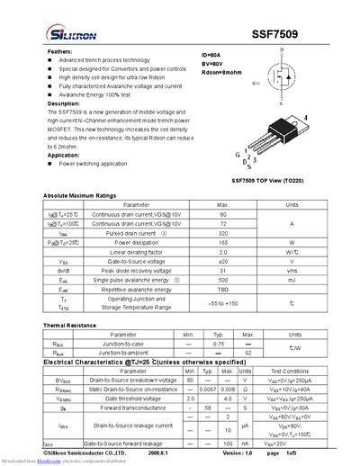
The SSF7509 is a middle‑voltage, high‑current N‑channel enhancement mode trench power MOSFET. It features an advanced trench process, high‑density cell design for ultra‑low RDS(on), and is fully characterized for avalanche voltage and current, making it suitable for power‑switching applications.
The document lists absolute maximum ratings, thermal resistance, electrical characteristics, gate charge data, and mechanical dimensions. Key parameters include a continuous drain current of 80 A, typical on‑resistance of 0.0067 Ω, breakdown voltage of 80 V, and a maximum power dissipation of 165 W.
| Continuous drain current (ID) @ 25°C, VGS=10V | 80 A |
|---|---|
| Gate threshold voltage (VGS(th)) typical | 4.0 V |
| Drain‑to‑Source breakdown voltage (BVDSS) | 80 V |
| Junction‑to‑case thermal resistance (RθJC) | 0.75 °C/W |
| Maximum power dissipation | 165 W |
| Total gate charge (Qg) | 100 nC |
| Input capacitance (Ciss) | 3200 pF |
The SSF7509 can handle a continuous drain current of 80 A at 25 °C with VGS=10 V.
The device’s drain‑to‑source breakdown voltage is rated at 80 V.