
This manual describes the functions, peripheral circuit design, parameter selection and layout guidelines for the SLM2304S HVIC gate driver used to drive up…
The SLM2304S HVIC gate driver from Shuming is designed for high‑voltage applications such as BLDC motors, high‑power DC‑DC converters, household appliances, stepper drivers and inverters. It integrates UVLO protection, interlock control and a bootstrap supply to ensure safe operation of high‑side MOSFETs/IGBTs.
Key design topics covered include UVLO threshold settings, interlock behavior, bootstrap capacitor and resistor selection, gate‑resistor calculation, and PCB layout recommendations to minimise parasitic inductance and EMI. Practical circuit examples and design equations are provided to help engineers implement reliable high‑side driver solutions. This manual is written in Chinese.
| Maximum drive voltage | 600 V |
|---|---|
| UVLO hysteresis voltage | 0.7 V |
| Typical VDD supply voltage | 12–15 V |
| Internal pull‑down resistance on HIN/LIN | ≈500 kΩ |
| Recommended bootstrap resistor value | 5–10 Ω |
| Recommended gate‑resistor (RGATE) calculation | RG = 1/(CISS·2π·fR·Q) |
UVLO shuts off the driver output when VCC/VBS falls below the low‑threshold (VCCUV‑/VBSUV) and re‑enables it only after the voltage rises above the high‑threshold (VCCUV+/VBSUV).
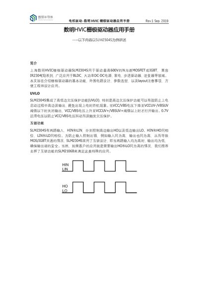
The interlock ensures that when both high‑side and low‑side inputs are high, both outputs are forced low to prevent shoot‑through of the MOSFET/IGBT pair.
Use a combination of an electrolytic capacitor (10–100 µF) and a 100 nF ceramic capacitor close to the VDD and COM pins.