
Datasheet for the Navitas NV6117 650 V GaNFast power IC in a 5 x 6 mm QFN package.
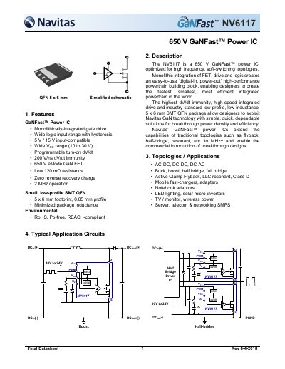
Navitas NV6117 is a 650 V GaNFast power IC optimized for high-frequency, soft-switching topologies. It monolithically integrates a GaN FET, gate drive, and logic in a 5 x 6 mm SMT QFN package.
Documented applications include AC-DC, DC-DC, and DC-AC conversion, buck, boost, half-bridge, full-bridge, active clamp flyback, LLC resonant, and Class D circuits. The datasheet covers absolute maximum ratings, recommended operating conditions, electrical characteristics, switching waveforms, pin functions, functional description, PCB layout, package outline, and ordering information.
| Drain-to-source voltage (absolute maximum) | -7 to +650 V |
|---|---|
| Transient drain-to-source voltage | 750 V |
| Maximum supply voltage (VCC) | 30 V |
| Recommended supply voltage (VCC) | 10 to 24 V |
| Continuous drain current | 12 A at TC = 100 C |
| Pulsed drain current | 24 A (10 us, TJ = 25 C); 16 A (10 us, TJ = 125 C) |
| Drain-source on-resistance | 120 mΩ typical, 170 mΩ maximum |
| Switching frequency | 2 MHz |
| Operating junction temperature | -40 to +125 C |
| Package | 5 x 6 mm QFN |
| Thermal resistance, junction-to-case | 1.8 C/W |
The absolute maximum drain-to-source voltage is 650 V.
The typical drain-source on-resistance is 120 mΩ, with a maximum of 170 mΩ.
It uses a 5 x 6 mm QFN package.
The recommended operating junction temperature range is -40 to +125 °C.