
This document provides a detailed description of the LTC4365 and LTC4365-1 voltage protection controllers.
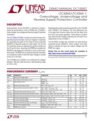
The DC1555C is a demonstration circuit from Linear Technology for the LTC4365 and LTC4365-1 overvoltage, undervoltage and reverse supply protection controllers. It includes the controller, two back-to-back connected power MOSFETs, three jumpers and three LEDs that indicate the input and output voltages and the FAULT pin signal.
The manual gives a performance summary with board input voltage range, supply current, gate drive and threshold specifications, explains the operating principles, and provides a quick start procedure for reverse voltage, undervoltage/overvoltage and jumper tests. A schematic diagram and board assembly information are also included.
| Board Input Voltage Range | –30V to 30V |
|---|---|
| Input Supply Undervoltage Lockout | 1.8V min, 2.2V typ, 2.4V max (VIN rising) |
| UV Input Threshold Voltage | 492.5mV min, 500mV typ, 507.5mV max (UV falling) |
| OV Input Threshold Voltage | 492.5mV min, 500mV typ, 507.5mV max (OV rising) |
| External N-Channel Gate Drive | 3V to 9.8V (GATE – VOUT) |
| SHDN Input Threshold | 0.4V min, 0.75V typ, 1.2V max |
| LTC4365/LTC4365-1 DC Voltage Withstand | –40V to +60V |
| Valid Operating Range | 2.5V to 34V |
| Supply Current (controller) | 10µA during shutdown, 125µA while operating |
| Gate Fault Recovery Delay | 36ms typ for LTC4365; 1ms for LTC4365-1 |
It is intended to demonstrate the performance of the LTC4365 and LTC4365-1 overvoltage, undervoltage and reverse supply protection controllers.
They can withstand DC voltages between –40V and +60V and have a valid operating range of 2.5V to 34V.
Their supply protection parameters are identical; they differ in the gate fault recovery delay time and the delay from turn-off to low-power operation.
The circuit on the DC1555C is optimized for 12V operation.