
This document describes the features and characteristics of the MB90350 series microcontrollers, which are especially designed for automotive and industrial applications. The main feature is the on-board CAN interface, which supports a flexible message buffer scheme and offers more functions than a normal full CAN approach. With the 0.35 µm CMOS technology, the microcontrollers have on-chip FLASH-ROM program memory up to 128 Kbytes. An internal voltage booster and voltage regulator provide advantages in terms of EMI and power consumption. The microcontrollers also feature a 4-channel Output Compare Unit, a 6-channel Input Capture Unit, and 2-channel UART for communication purposes.
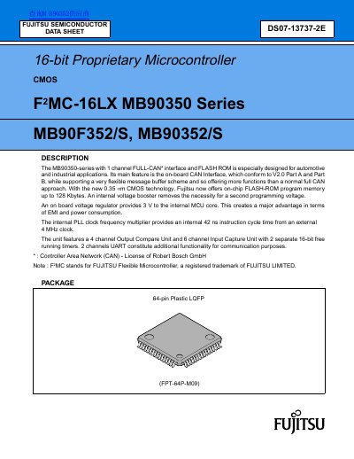
This document is a datasheet for the Fujitsu MB90350 Series, a 16-bit proprietary microcontroller (MCU) based on the F2MC-16LX CPU system. The series is specifically designed for automotive and industrial applications, featuring an on-board CAN interface compliant with V2.0 Part A and Part B, and up to 128 Kbytes of on-chip FLASH-ROM program memory.
Key features include a 0.35 mm CMOS technology with an internal voltage regulator to reduce EMI and power consumption, and a PLL clock frequency multiplier allowing for a 42 ns instruction cycle time from a 4 MHz external clock. The MCU supports various low-power modes, including Sleep, Watch, and Stop modes, and offers extensive I/O capabilities including UART, I2C, and multiple timers and timers.
| CPU System | F2MC-16LX |
|---|---|
| Instruction cycle time | 42 ns |
| ROM Memory | 128 Kbytes |
| Operating voltage range | 3.5 V - 5.5 V |
| Temperature range | -40 °C to +105 °C |
| Package | 64-pin Plastic LQFP |
| CAN Interface | 1 channel |
| A/D Converter | 15 channels |
Its main feature is the on-board CAN Interface, which conforms to V2.0 Part A and Part B.
The minimum instruction execution time is 42 ns when operating with a 4-MHz oscillation clock and 6-time multiplied PLL clock.