
The document describes the features and characteristics of the high-speed CMOS triple buffer 74V2G70, which was released on June 1, 2003. These features include high-speed transmission, low power consumption, high noise immunity, power down protection on inputs and outputs, symmetrical output impedance, balanced propagation delays, and operating voltage range.
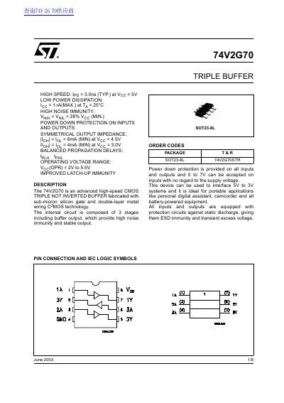
The 74V2G70 is an advanced high-speed CMOS triple not inverted buffer fabricated with sub-micron silicon gate and double-layer metal wiring technology. The internal circuit consists of three stages including a buffer output, providing high noise immunity and stable output. Power down protection is provided on all inputs and outputs, allowing 0 to 7V to be accepted on inputs regardless of the supply voltage.
| Operating Voltage Range | 2V to 5.5V |
|---|---|
| Propagation Delay Time (Typ) | 3.0ns |
| Quiescent Supply Current (Max) | 1 µA |
| Noise Immunity | 28% VCC |
| Output Impedance (Min) | 8 mA |
| Package Type | SOT23-8L |
The operating voltage range is 2V to 5.5V.
Yes, power down protection is provided on all inputs and outputs.
Yes, this device can be used to interface 5V to 3V systems.