
NC7SP02 is a single 2-Input NOR Gate from Fairchild’s Ultra Low Power (ULP) series of TinyLogic ULP 2-Input NOR Gate, ideal for applications where battery life is critical. This product is designed for ultra low power consumption within the VCC operating range of 0.9V to 3.6V VCC. The internal circuit is composed of a minimum of inverter stages, including the output buffer, to enable ultra low static and dynamic power. NC7SP02, for lower drive requirements, is uniquely designed for optimized power and speed, and is fabricated with an advanced CMOS technology to achieve best in class speed operation while maintaining extremely low CMOS power dissipation.
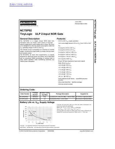
The NC7SP02 is a single 2-Input NOR gate designed for Ultra Low Power (ULP) applications where battery life is critical. It is fabricated with advanced CMOS technology to achieve best-in-class speed while maintaining extremely low power dissipation. The device operates within a supply voltage range of 0.9V to 3.6V and includes patented Quiet Series noise/EMI reduction circuitry.
| Supply Voltage | 0.9V to 3.6V |
|---|---|
| Operating Temperature | -65°C to +150°C |
| Propagation Delay (Typ) | 3 ns |
| Static Drive Current | 42.6 mA |
| Package Options | 5-Lead SC70, 6-Lead MicroPak |
The device supports a supply voltage operation from 0.9V to 3.6V.
Yes, it is 3.6V overvoltage tolerant I/O's at Vcc from 0.9V to 3.6V.
The typical propagation delay is 3 ns for a supply voltage of 3.0V to 3.6V.