
The document provides information about the I/O pins and functions of the EP20K200E chip.
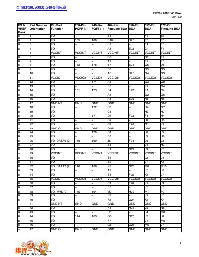
This document details the I/O pin assignments for the EP20K200E FPGA. It lists the pad numbers and functions for different package variants, including 208-Pin PQFP, 240-Pin IPQFP, 484-Pin FineLine BGA, 356-Pin BGA, 652-Pin BGA, and 672-Pin BGA.
The table specifies the Bank, VREF, Orientation, and Function for each pin. Functions include power supplies (VCCINT, VCCIO, GND), control signals (CONF_DONE, NSTATUS), and various logic and timing pins (DATA, CLK, TDI, TCK, TMS).
| Supported Packages | 208-Pin PQFP, 240-Pin IPQFP, 484-Pin FineLine BGA, 356-Pin BGA, 652-Pin BGA, 672-Pin BGA |
|---|
The supported packages are 208-Pin PQFP, 240-Pin IPQFP, 484-Pin FineLine BGA, 356-Pin BGA, 652-Pin BGA, and 672-Pin BGA.
Pad 201 on the 208-Pin PQFP package is CONF_DONE.
Pad 213 on the 208-Pin PQFP package is TCK.
Pad 214 on the 208-Pin PQFP package is TMS.