
This document describes the arrangement and function of the I/O pins and VREF voltage pins of the EP20K1000E chip. The chip has three versions, namely 652-pin BGA, 672-pin FineLine BGA, and 1020-pin FineLine BGA.
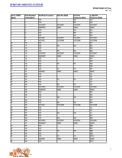
This document serves as a reference guide for the EP20K1000E FPGA, specifically focusing on the I/O pin configurations. It lists the pad numbers, bank orientations, and specific functions for various pins across different package types.
The data is organized by package size, covering the 652-Pin, 672-Pin, and 1020-Pin FineLine BGA variants. Each entry maps a pad number to its function, such as power supplies (VCCINT, VCCIO), ground connections (GNDINT, GNDIO), and specific I/O signals like DATA, CLK, and control lines (nCS, nRS).
| Package Types | 652-Pin BGA, 672-Pin BGA, 1020-Pin BGA |
|---|---|
| Package Type | FineLine BGA |
| Document Version | ver. 1.0 |
Pad 356 is designated for the CONF_DONE function.
Pad 365 is designated for the TCK function.
Pad 366 is designated for the TMS function.