
This datasheet is about MC74AC273/74ACT273, which is a device with eight edge-triggered D-type flip-flops with individual D inputs and Q outputs.
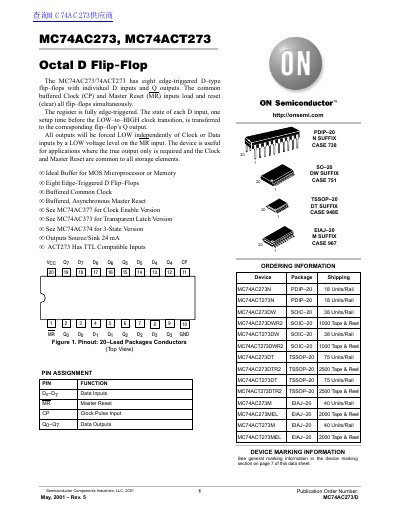
The MC74AC273 and MC74ACT273 are octal D-type flip-flops featuring eight edge-triggered storage elements with individual D inputs and Q outputs. These devices include a common buffered Clock (CP) input and a Master Reset (MR) input that allows for the simultaneous loading and resetting of all flip-flops. The register is fully edge-triggered, transferring the state of each D input to the corresponding Q output on the LOW-to-HIGH clock transition. All outputs are forced LOW independently of the Clock or Data inputs by applying a LOW voltage level to the MR input.
| Number of Flip-Flops | Eight |
|---|---|
| Outputs Source/Sink Current | 24 mA |
| Supply Voltage (AC) | 2.0 to 6.0 V |
| Supply Voltage (ACT) | 4.5 to 5.5 V |
| Maximum Operating Temperature | +85 °C |
| Maximum Clock Frequency (AC) | 125 MHz |
| Maximum Clock Frequency (ACT) | 200 MHz |
A LOW voltage level on the MR input forces all outputs LOW independently of the Clock or Data inputs.
The register is fully edge-triggered, transferring data on the LOW-to-HIGH clock transition.
Yes, the MC74ACT273 version has TTL compatible inputs.