
THC63LVD824 is a single and dual link LVDS receiver that supports single link transmission and dual link transmission. It supports SXGA+ and UXGA resolutions. It converts LVDS data streams back into 48 bits of CMOS/TTL data with falling edge or rising edge clock for convenience with a variety of LCD panel controllers.
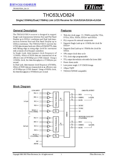
The THC63LVD824 is an LVDS receiver designed for flat panel displays, supporting Single Link transmission up to SXGA+ and Dual Link up to UXGA. It converts LVDS data streams into 48-bit CMOS/TTL data with programmable clock edges.
Key features include a wide dot clock range from 25MHz to 170MHz, an integrated PLL requiring no external components, and selectable TTL output driver capability for lower EMI. The device operates on a single 3.3V power supply.
| Single Link Clock Frequency | 135MHz |
|---|---|
| Dual Link Clock Frequency | 85MHz |
| Single Link Data Rate | 945Mbps per LVDS channel |
| Dual Link Data Rate | 595Mbps per LVDS channel |
| Dot Clock Range | 25-170MHz |
| Power Supply Voltage | 3.3V CMOS |
| Package Type | 100pin TQFP |
It supports Single Link up to SXGA+ and Dual Link up to UXGA.
No, the internal PLL requires no external components.