
This document describes the features and characteristics of Altera Corporation's FLEX 8000 programmable logic device family. This family of devices is a low-cost, high-density, register-rich CMOS programmable logic device, with system-level features such as in-circuit reconfigurability, PCI compliance, and JTAG boundary-scan test circuitry compliant with IEEE Std. 1149.1-1990. Additionally, the devices in this family have flexible interconnect, powerful I/O pins, and low power consumption.
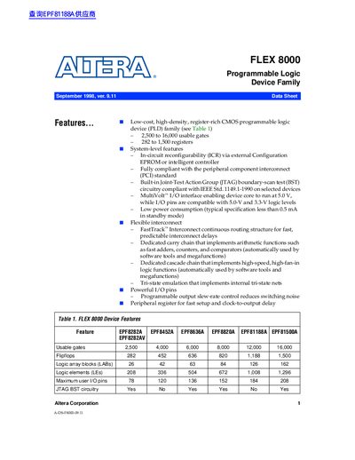
The Altera FLEX 8000 family combines the benefits of erasable programmable logic devices (EPLDs) and field-programmable gate arrays (FPGAs). These devices are ideal for applications such as digital signal processing, bus interfaces, and high-speed controllers. They feature a large number of storage elements and are fabricated on an advanced SRAM process.
| Usable gates | 2,500 to 16,000 |
|---|---|
| Registers | 282 to 1,500 |
| Standby power consumption | less than 0.5 mA |
| I/O compatibility | 5.0-V and 3.3-V |
| Pin count | 84 to 304 pins |
It is a family of low-cost, high-density, register-rich CMOS programmable logic devices.
They can be reconfigured in-circuit by resetting the device and loading new data, requiring less than 100 ms.
The Altera MAX+PLUS II development system provides schematic, text, waveform design entry, and device programming support.