
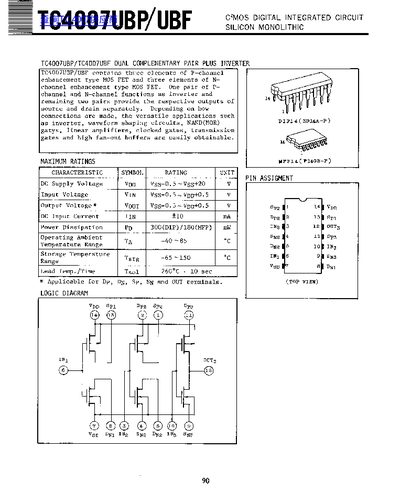
This document is a technical datasheet for the TC4007UBP/TC4007UBF CMOS digital integrated circuit. The device contains three P-channel and three N-channel enhancement type MOS FET elements configured to function as an inverter, source output, and drain output.
| DC Supply Voltage | -0.5 to 20 V |
|---|---|
| Input Voltage | -0.5 to +0.5 V beyond supply rails |
| Power Dissipation (DIP) | 300 mW |
| Operating Ambient Temperature | -40 to +85 C |
| DC Supply Voltage (Recommended) | 3 - 18 V |
The device can be used in inverter, waveform shaping circuits, NAND/NOR gates, linear amplifiers, clocked gates, transmission gates, and high fan-out buffers.
The device can handle a DC supply voltage ranging from -0.5V to +20V.
The maximum power dissipation is 300 mW for DIP packages and 180 mW for MFP packages.
The circuit operates within an ambient temperature range of -40°C to +85°C.