
Eon Silicon Solution, Inc. introduced the EN29F040A 4-Megabit flash memory in 2003. The flash supports fast read, write, and erase operations. It uses a 0.23-micron triple-metal double-poly triple-well CMOS flash technology with a 100K endurance cycle and is available in commercial and industrial temperature ranges.
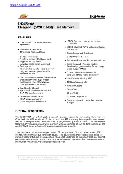
The document describes the LON EN29F040A, an electrically erasable read/write non-volatile flash memory organized into eight uniform sectors of 64Kbytes each. It supports a 5.0V operating voltage for read, write, and erase operations with access times as fast as 45ns.
Key features include hardware locking for sector protection, low standby current (1pA CMOS), and support for JEDEC standard program and erase commands. The device is available in various packages including 32-pin PDIP, PLCC, and TSOP.
| Memory Capacity | 4 Megabit (512K x 8-bit) |
|---|---|
| Operating Voltage | 5.0V |
| Read Access Time | 45ns, 55ns, 70ns, and 90ns |
| Sector Size | 64Kbytes each |
| Program Time (Byte) | 10us typical |
| Erase Time (Chip) | 3.5s typical |
| Standby Current (CMOS) | 1pA typical |
| Active Read Current | 30mA |
| Endurance Cycle | 100K |
The 4M of memory is arranged in eight uniform sectors of 64Kbytes each.
Yes, it supports hardware locking of sectors to prevent program or erase operations within individual sectors.
The device is available in 32-pin PDIP, 32-pin PLCC, and 32-pin TSOP (Type 1) packages.