
OR2 Series 2 Field-Programmable Gate Arrays Data Sheet
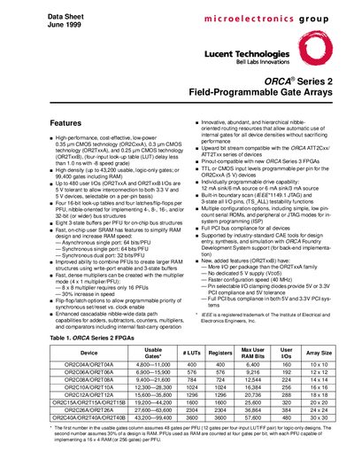
This document is a technical datasheet for the ORCA Series 2 family of SRAM-based Field-Programmable Gate Arrays (FPGAs) manufactured by Lucent Technologies. The devices utilize advanced CMOS technologies ranging from 0.35 um to 0.25 um, offering high performance with low power consumption and logic-only gate delays under 1.0 ns.
The architecture consists of Programmable Logic Cells (PLCs) surrounded by Programmable Input/Output Cells (PICs). Key features include up to 480 user I/Os, support for both 3.3 V and 5 V systems, full PCI bus compliance, and compatibility with industry-standard CAE tools. The datasheet details device specifications, timing characteristics, configuration modes, and package information.
| Technology Node | 0.35 um, 0.3 um, or 0.25 um CMOS |
|---|---|
| Max Usable Logic Gates | 43,200 (logic-only) or 99,400 (including RAM) |
| Max User I/Os | 480 |
| LUTs per PFU | Four 16-bit look-up tables |
| Max Speed Grade Delay | < 1.0 ns |
| Bus Compliance | Full PCI bus compliance |
The series uses 0.35 um, 0.3 um, and 0.25 um CMOS technologies depending on the specific model.
Yes, the pinout is compatible with new ORCA Series 3 FPGAs.
Yes, OR2TxxA and OR2TxxB I/Os are 5 V tolerant to allow interconnection to both voltages.