
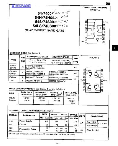
This document provides the connection diagrams and pinout tables for the 54/7400, 54H/74H00, 54S/74S00 and 54LS/74LS00 quad 2‑input NAND gate families. It includes commercial and military grade package options and their corresponding pin assignments.
Electrical specifications such as input high/low thresholds, output high/low levels, propagation delay, power‑supply voltage and current limits are listed for each family, together with temperature operating ranges.
| Input HIGH voltage (54/7400) | 1.0 V |
|---|---|
| Input LOW voltage (54/7400) | 1.0 V |
| Output HIGH voltage (54/7400) | 20 V |
| Output LOW voltage (54/7400) | 10 V |
| Power‑supply voltage (54/7400) | 16.8 V |
| Supply current (54/7400) | 40 mA |
The document provides two pinout configurations, Pinout A and Pinout B, for the 54/7400 series devices.