
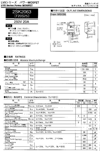
The 2SK2063 (F20S25) is a LVX series N‑channel power MOSFET designed for high‑voltage, high‑current applications. The document provides absolute maximum ratings, electrical characteristics, and thermal data for the device.
Key specifications include a 250 V drain‑source voltage, 7 A continuous drain current, 65 W total power dissipation, and an on‑state resistance of 0.025 Ω. Capacitance values, gate‑source voltage limits, and thermal resistance are also listed.
| Drain‑Source Voltage (V_DSS) | 250 V |
|---|---|
| Continuous Drain Current (I_D) | 7 A |
| Peak Drain Current | 40 A |
| Total Power Dissipation (P_D) | 65 W |
| On‑state Resistance (R_DS(on)) | 0.025 Ω |
| Gate‑Source Voltage (V_GS) | +30 V |
| Input Capacitance (C_iss) | 1,200 pF |
| Cutoff Capacitance (C_oss) | 465 pF |
| Thermal Resistance (Junction‑to‑Case) | 1.92 °C/W |
The device is rated for a maximum drain‑source voltage of 250 V.
It can continuously conduct up to 7 A of drain current.
The total power dissipation rating is 65 W.
The gate‑source voltage is limited to +30 V.