
This document introduces the features of CY7C1411AV18, CY7C1426AV18, CY7C1413AV18 and CY7C1415AV18 4-Word Burst Architecture SRAM
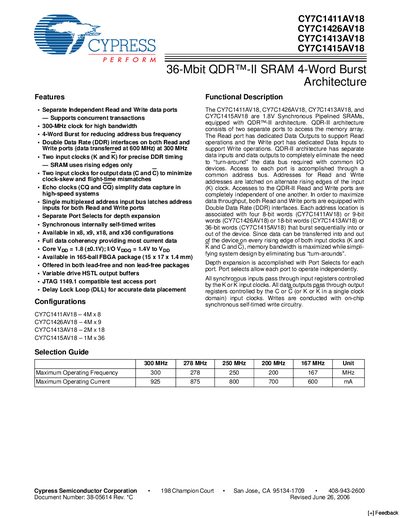
The CY7C1411AV18, CY7C1426AV18, CY7C1413AV18 and CY7C1415AV18 are synchronous pipelined QDR‑II SRAMs with separate read and write ports, DDR interfaces and up to 300 MHz clock operation. Each device uses a 165‑ball FBGA package and offers depth‑expansion via independent port‑select inputs.
The document includes detailed pin configurations, timing tables, and descriptions of read/write operations, single‑clock mode, concurrent transactions, programmable impedance, and echo‑clock functionality, enabling designers to integrate these high‑speed memory devices into their systems.