
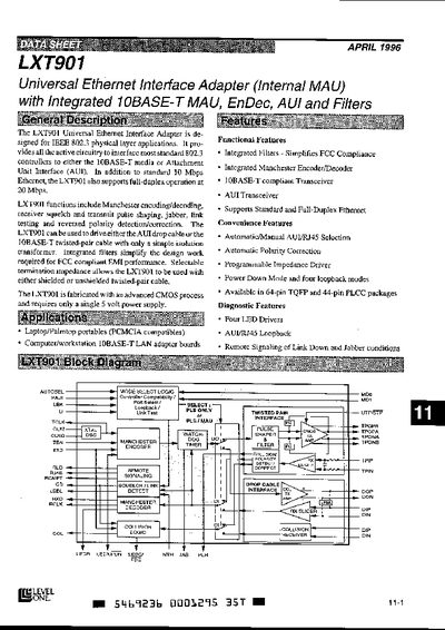
The LXT901 is a universal Ethernet interface adapter designed for IEEE 802.3 physical‑layer applications. It provides all active circuitry needed to connect standard 802.3 controllers to either 10BASE‑T twisted‑pair or AUI drop cables, supporting 10 Mbps Ethernet and full‑duplex 20 Mbps operation. Integrated Manchester encoder/decoder, automatic polarity correction, and selectable termination impedance simplify board design and ensure FCC‑compliant EMI performance.
The device includes four LED drivers for status indication, programmable impedance drivers, and multiple loopback and test modes. It is available in 64‑pin TQFP and 44‑pin PLCC packages and operates from a single 5 V supply. Detailed pin descriptions, controller‑compatibility modes, and timing diagrams are provided for designers.
| Supported Ethernet Speeds | 10 Mbps (half‑duplex) and 20 Mbps full‑duplex |
|---|---|
| Package Options | 64‑pin TQFP and 44‑pin PLCC |
| Integrated Filters | Simplify FCC‑compliant EMI performance |
| LED Drivers | Four open‑drain drivers (receive, transmit, link, collision) |
| Clock Output | 10 MHz transmit clock (TCLK) |
| Crystal Requirement | 20 MHz crystal (or external 20 MHz clock) |
It automatically detects reversed polarity and corrects it, indicating the condition on the PLR pin.
The device is offered in 64‑pin TQFP and 44‑pin PLCC packages.
Link integrity testing is enabled by tying pin 8 (LD) high; the chip then transmits test pulses and enters a link‑fail state if no pulses are detected within 50‑150 ms.