
This data sheet provides the features and specifications of the UT63M1XX MIL-STD-1553A/B bus transceiver.
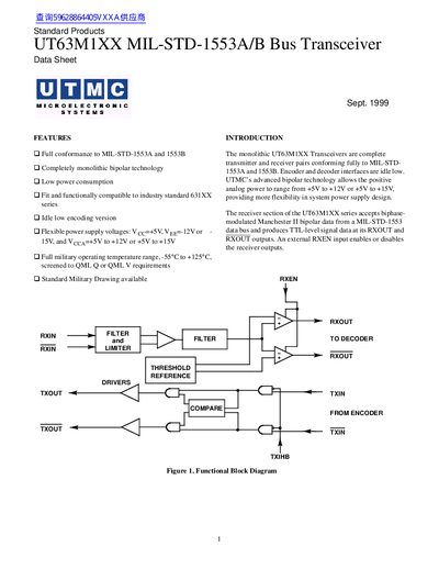
The UT63M1XX series are monolithic MIL-STD-1553A/B bus transceivers offering full conformance to the standard, low power consumption, and flexible power‑supply options. They are available in single‑channel (24‑pin) and dual‑channel (36‑pin) packages and support both short‑stub (direct‑coupled) and long‑stub (transformer‑coupled) bus connections.
Key features include idle‑low encoding, a wide operating temperature range from –55 °C to +125 °C (junction up to +150 °C), and selectable supply voltages (+5 V to +12 V or +5 V to +15 V for VCCA, –12 V or –15 V for VEE). The datasheet details pin assignments, electrical limits, absolute maximum ratings, and ordering information for the UT63M105, UT63M107, UT63M125, and UT63M127 variants.
| Supply voltage options | VCC +5 V, VEE –12 V or –15 V, VCCA +5 V to +12 V or +5 V to +15 V |
|---|---|
| Operating temperature (junction) | -55 °C to +150 °C |
| Operating temperature (case) | -55 °C to +125 °C |
| Input voltage range (receiver) | 0 to +5 V (logic), 42 Vpp differential |
| Transmitter output current | 190 mA |
| Power dissipation per channel | 4 W |
The device can be powered with VCC +5 V, VEE –12 V or –15 V, and VCCA selectable between +5 V to +12 V or +5 V to +15 V.
The junction temperature range is –55 °C to +150 °C, while the case temperature range is –55 °C to +125 °C.
In the single‑channel (24‑pin) package, TXOUT and TXOUT are differential outputs, TXIN and TXIN are complementary TTL inputs, RXOUT and RXOUT are complementary TTL outputs, and RXIN and RXIN are differential inputs.