
GS8322V18/36/72 is a 37,748,736-bit high performance synchronous SRAM with a 2-bit burst address counter. Although of a type originally developed for Level 2 Cache applications supporting high performance CPUs, the device now finds application in synchronous SRAM applications, ranging from DSP main store to networking chip set support.
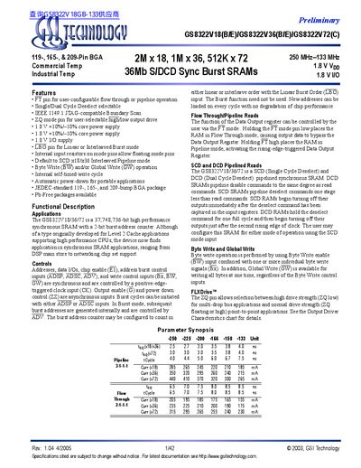
The GS8322V series from GSI Technology provides high‑performance synchronous burst SRAMs for Level‑2 cache, DSP main store, and networking chip‑set applications. The devices are offered in three capacities – 2 M × 18, 1 M × 36, and 512 K × 72 bits – and support both pipeline and flow‑through read modes.
Key features include IEEE 1149.1 JTAG‑compatible boundary‑scan, selectable FT (Flow‑Through/Pipeline) mode, ZQ pin for high/low drive strength, automatic power‑down, and both byte‑write (BW) and global‑write (GW) operations. The parts are supplied in 119‑, 165‑, and 209‑pin BGA packages and operate from a 1.8 V core supply over commercial and industrial temperature ranges.
| Capacities | 2M × 18, 1M × 36, 512K × 72 |
|---|---|
| Maximum operating frequency | 250 MHz (pipeline) – 133 MHz (flow‑through) |
| Core supply voltage | 1.8 V |
| I/O supply voltage | 1.8 V |
| Package types | 119‑, 165‑, 209‑pin BGA |
| Temperature range | Commercial and Industrial |
| Write modes | Byte Write (BW) and Global Write (GW) |
| Power‑down feature | Automatic power‑down for portable applications |
The FT pin selects Flow‑Through mode (low) or Pipeline mode (high) for the SRAM’s data output path.
The SRAM includes an automatic power‑down feature that activates when the device is idle.
Both Byte Write (BW) using individual byte enable pins and Global Write (GW) to write all bytes simultaneously are supported.
The ZQ pin selects high‑drive strength for multi‑drop bus applications or normal drive strength for point‑to‑point connections.