
PPLN microchip user manual
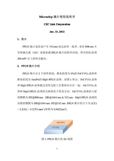
The PPLN microchip is a single‑component device that converts 808 nm pump light into green light at 532 nm. It consists of a Nd:YVO4 crystal and a MgO:PPLN crystal bonded together with optical glue. The chip dimensions are 2 mm × 2.2 mm × 0.5 mm.
To build a green‑laser source, the chip is combined with an 808 nm semiconductor pump laser (c‑mount or f‑mount), a thermoelectric cooler, heat sink, thermistor, and metal hardware. The pump laser should be positioned 0.5–1 mm from the chip, with the crystal axis aligned vertically. Proper alignment yields green output power exceeding 200 mW when using a 1.5 W pump laser. This manual is written in Chinese.
| Volume | 0.0022 cm³ |
|---|---|
| Input surface coating | HT@808 nm, HR@1064 nm |
| Output surface coating | HR@1064 nm, HT@532 nm |
| Green output power (with 1.5 W pump) | >200 mW |
When pumped with a 1.5 W 808 nm laser, the chip can produce more than 200 mW of 532 nm green light.
The distance should be kept between 0.5 mm and 1 mm.