
The SN74LVC2G00 is a dual 2-input positive-NAND gate designed for 1.65V to 5.5V VCC operation. It supports 5V VCC operation and inputs accept voltages up to 5.5V. The maximum propagation delay is 4.3ns at 3.3V. It has low power consumption, with a maximum ICC of 10μA. The output drive is ±24mA at 3.3V. The typical output ground bounce voltage (VOLP) is less than 0.8V at VCC = 3.3V, TA = 25°C, and the typical output VOH undershoot voltage (VOHV) is greater than 2V at VCC = 3.3V, TA = 25°C. It supports partial-power-down mode operation, with Ioff current. The latch-up performance exceeds 100mA per JESD 78, Class II. ESD protection exceeds JESD 22, with a 2000V human-body model (A114-A) and 1000V charged-device model (C101).
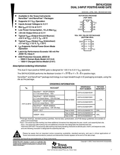
The SN74LVC2G00 is a dual 2‑input positive‑NAND gate designed for 1.65 V to 5.5 V operation. It offers low power consumption, high‑speed switching (max 4.3 ns propagation delay at 3.3 V) and robust ESD protection.
The document provides detailed ordering information, recommended operating conditions, electrical and switching characteristics, mechanical drawings for the NanoStar, NanoFree, DCT and DCU packages, and an important notice about product warranties and revisions.
| Maximum propagation delay (tpg) | 4.3 ns at 3.3 V |
|---|---|
| Output drive current | +24 mA at 3.3 V |
It can source or sink up to +24 mA at a 3.3 V supply.
The propagation delay is up to 4.3 ns when powered at 3.3 V.