
KK74VHC373 is an octal D-type latch with three-state outputs. It is designed for use in modern high-performance computers and electronic equipment for consumer applications. The high-level KK74VHC373 is identical in pinout to the IC series KK74HC373A, KK74HCT373A, KK74AC373A, KK74ACT373A. The input voltage levels are compatible with standard C-MOS levels. The output voltage levels are compatible with input levels of C-MOS, N-MOS, and TTL ICs.
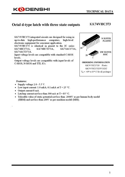
The KK74VHC373 is an octal D‑type latch with three‑state outputs designed for use in high‑performance computers and consumer electronic equipment. It is pin‑compatible with the KK74HC373A, KK74HCT373A, KK74AC373A, and KK74ACT373A families and operates from a 2.0 V to 5.5 V supply.
The document lists detailed electrical parameters, including absolute maximum ratings, DC and AC characteristics, and timing diagrams for both input and output pulses. Package dimensions for both plastic DIP and SOIC versions are also provided.
| Supply voltage | 2.0 V – 5.5 V |
|---|---|
| Low input current | 1.0 µA; 0.1 µA at 25 °C |
| Output current | 8 mA |
| Latchup current (min) | 300 mA at 85 °C |
| Absolute max supply voltage | -0.5 V – 7.0 V |
The device operates with a supply voltage from 2.0 V to 5.5 V.
Each output can source up to 8 mA.
Pin 1 is Output Enable (OE), pins 2‑9 are data inputs/outputs, pin 10 is GND, and pins 11‑20 include LE, Q0‑Q7, and supply.
Absolute maximum ratings include a supply voltage of –0.5 V to 7.0 V and an input voltage of –0.5 V to 7.0 V.