
This datasheet provides detailed information on NL37WZ14's features and characteristics, including operating voltage range, input/output current, output logic levels, and package dimensions.
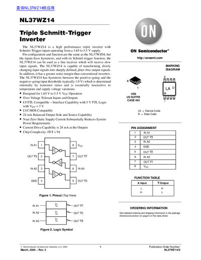
The NL37WZ14 triple Schmitt‑Trigger inverter from ON Semiconductor provides hysteresis‑enhanced inputs, allowing slow signals to be converted into clean, jitter‑free outputs. It operates from a 1.65 V to 5.5 V supply and offers over‑voltage‑tolerant inputs, LVTTL and LVCMOS compatibility, and a 24 mA balanced output sink/source capability.
The datasheet details maximum ratings, recommended operating conditions, DC and capacitive characteristics, pin assignments, and package dimensions. Ordering information and mechanical drawing data are also included for design and procurement.
| Supply Voltage (Operating) | 2.3 V – 5.5 V |
|---|---|
| Input Voltage (Operating) | 0 V – 5.5 V |
| Output Sink Current | +50 mA |
| Power Dissipation (85 °C, still air) | 250 mW |
| Storage Temperature Range | -65 °C – +150 °C |
| Typical Positive Input Threshold (V+) | 1.0 V |
The device operates with a supply voltage from 2.3 V to 5.5 V.
It can sink up to +50 mA at the output.
The typical positive input threshold is about 1.0 V.
It can be stored from –65 °C up to +150 °C.