
The SN74LVC2G04 is a dual input inverter from Texas Instruments. It operates over a voltage range of 1.65V to 5.5V, has an input voltage range of 5.5V, a maximum propagation delay of 4.1ns, static power consumption of 10µA, an output drive current of 24mA, a typical output ground bounce voltage of less than 0.8V, a typical output VOH undershoot of greater than 2V, supports partial power-down mode, latch-up performance exceeds 100mA, ESD protection exceeds JESD22, and supports 2000V human body model (A114-A), 200V machine model (A115-A), and 1000V charged device model (C101).
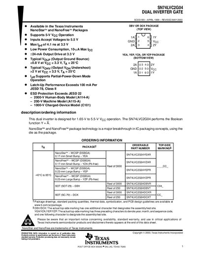
The SN74LVC2G04 is a dual inverter gate designed for 1.65 V to 5.5 V supply operation. It offers low power consumption, high‑speed switching, and partial‑power‑down capability. The device is available in several advanced NanoStar™ and NanoFree™ wafer‑level packages as well as traditional DBV and DCK surface‑mount packages.
The data sheet provides detailed electrical characteristics, recommended operating conditions, mechanical dimensions, and ordering information. It also includes safety notices, warranty statements, and references to TI application notes for proper usage.
| Output high‑level voltage (VOH) typical | 2.4 V at IOH = –16 mA |
|---|
Typical propagation delay ranges from about 1.2 ns to 3.2 ns depending on supply voltage.