
The NLU1G08 is a high-speed CMOS 2-input AND gate with an ultra-small footprint. It features high speed, low power dissipation, and overvoltage protection.
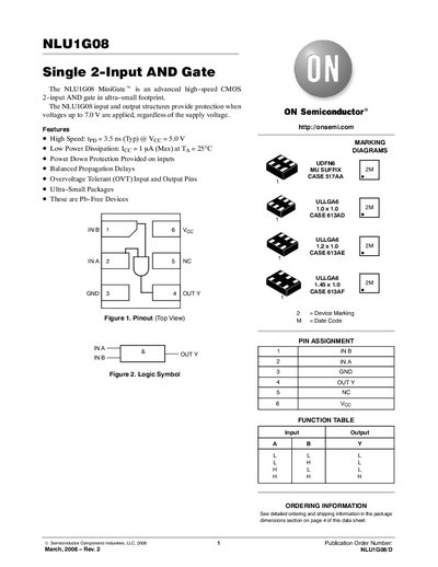
The NLU1G08 MiniGate™ is a high‑speed CMOS 2‑input AND gate featuring a typical propagation delay of 3.5 ns at 5 V, low power dissipation of 1 µA, and over‑voltage tolerant input and output pins. It operates over a wide voltage range (‑0.5 V to +7.0 V) and provides up to 125 mA source/sink current.
Electrical specifications include maximum ratings for supply and input voltages, storage temperature from –65 °C to +150 °C, and detailed package dimensions for the ultra‑small UDFN6 (1.0 × 1.0 mm) footprint. Ordering information, pin assignments, and legal notices are also provided.
| Typical propagation delay (tpp) | 3.5 ns @ Vcc=5.0 V |
|---|---|
| Maximum supply current (Icc) | 1 µA (max) at 25 °C |
| Input/Output voltage range | -0.5 V to +7.0 V |
| Output source/sink current | 125 mA (max) |
| Storage temperature range | -65 °C to +150 °C |
| Over‑voltage tolerant I/O | Yes |
The typical propagation delay is 3.5 ns at a 5 V supply.
It supports input voltages from –0.5 V to +7.0 V.
Yes, the device has over‑voltage tolerant (OVT) input and output pins.